
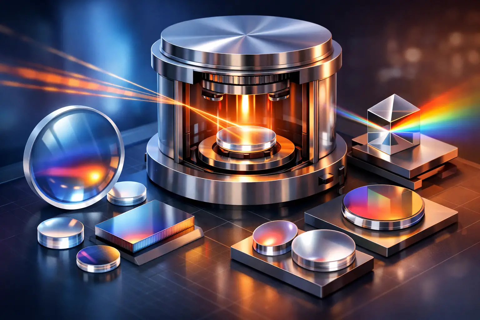
A high-value optic can fail its intended function because of a film only a few nanometres too thin, a refractive-index shift at the edge of tolerance, or local stress that changes the substrate figure. Precision optics sputtering addresses these risks by depositing functional thin films under tightly controlled vacuum conditions. For manufacturers of lenses, filters, mirrors, sensors and laser components, the process is not merely a finishing stage. It is a decisive factor in optical performance, service life and production yield.
What precision optics sputtering controls
Sputtering is a physical vapour deposition process in which energetic ions release atoms from a solid target. These atoms travel through a vacuum chamber and condense on the component surface as a thin film. In optical applications, the deposited materials can include metals, oxides, nitrides and other compounds selected for their optical, electrical or protective properties.
The term precision matters because an optical coating must meet several requirements at once. Thickness determines interference behaviour. Refractive index and extinction coefficient influence transmission, reflection and absorption. Film density, roughness and stress affect durability, scatter and the mechanical condition of the substrate. A coating that performs well at the centre of a witness sample may still be unsuitable if its characteristics vary across a large optic, a curved surface or a production batch.
Magnetron sputtering is frequently chosen where stable deposition rates, controlled film properties and industrial repeatability are required. Reactive sputtering extends the process window by introducing gases such as oxygen or nitrogen, enabling dielectric materials to be formed from metallic targets. This is technically valuable, but it increases the importance of gas control, plasma stability and feedback systems. Small deviations in reactive conditions can alter film stoichiometry and therefore shift the optical response.
Optical performance is designed layer by layer
An optical thin-film stack is a calculated system rather than a single material choice. Anti-reflection coatings reduce reflection across a specified wavelength range. High-reflection stacks use alternating layers of differing refractive index to achieve defined reflectance. Bandpass filters transmit a narrow spectral range while rejecting adjacent wavelengths. Protective conductive films may combine optical transmission with electromagnetic shielding or electrical functionality.
The layer design provides only the theoretical starting point. The deposited film must reproduce that design on the real component. This requires precise control of target power, pressure, gas flow, substrate movement, deposition time and temperature. The process also needs to account for substrate material and geometry. Fused silica, optical glass, sapphire, polymers and semiconductor materials do not respond identically to thermal load, plasma exposure or film stress.
For demanding optical assemblies, coating development therefore begins with the functional requirement: wavelength range, angle of incidence, polarisation, environmental exposure and allowed loss. Mechanical interfaces and subsequent assembly steps are equally relevant. A coating designed for excellent spectral performance may be the wrong choice if it cannot tolerate cleaning chemicals, humidity cycling, sterilisation or bonding processes.
Uniformity is more than a thickness map
Thickness uniformity is often expressed as a percentage across a substrate. This is useful, but not sufficient for precision optics. On a multilayer stack, a small local thickness deviation can cause a meaningful shift in cut-on wavelength, peak transmission or reflected colour. The effect depends on the layer count, material contrast and spectral specification.
Uniformity is influenced by the source-to-substrate geometry, target erosion profile, substrate rotation, planetary motion and masking concept. Large-format optics and non-planar components require particular attention. A process that is suitable for a small flat wafer may not transfer directly to a curved lens, a prism or a cylindrical optical element.
The same applies to batch loading. Component position, carrier design and available line of sight determine the coating distribution. Establishing repeatable loading patterns is therefore part of process engineering, not an administrative detail. For serial production, validated fixtures and defined handling procedures can contribute as much to consistency as the vacuum system itself.
Film density, stress and surface quality
Optical coatings interact with light at their interfaces. Surface roughness, particle contamination and microstructural defects can increase scatter and reduce transmission. Dense films tend to offer better resistance to moisture penetration and environmental ageing than porous structures, although the optimum structure depends on material system and application.
The energy of arriving species has a major effect on film growth. Process pressure, plasma conditions and substrate bias can be adjusted to influence density, adhesion and morphology. However, more energetic deposition is not automatically better. Sensitive substrates may suffer from excessive heating, charge-related effects or stress. Polymer optics, bonded assemblies and components with pre-existing functional layers require a carefully limited process load.
Stress must be assessed in context. Compressive or tensile stress can bend thin substrates, alter the surface figure of precision mirrors or cause adhesion problems in complex layer systems. Managing stress may involve material selection, deposition parameters, layer architecture and, where permissible, thermal treatment. The appropriate strategy depends on the substrate thickness, optical tolerance and operational environment.
Process monitoring turns specification into repeatability
A coating specification is credible only when the process can demonstrate repeatability. In precision optics sputtering, this begins with a clean and controlled vacuum environment. Chamber condition, target history, base pressure and contamination management affect film quality from one run to the next.
During deposition, rate monitoring and optical control support accurate layer termination. Quartz crystal monitoring can provide a deposition-rate reference, while optical monitoring observes changes in transmission or reflection during growth. The most effective approach depends on the optical design, material transparency and required tolerance. For critical multilayer systems, combining monitoring methods may provide greater confidence than relying on a single signal.
Post-process verification should reflect the component’s actual function. Spectrophotometric measurements confirm transmission and reflectance over the relevant spectral range. Additional inspection may address coating appearance, adhesion, environmental resistance, thickness distribution, surface defects and substrate distortion. In regulated sectors, traceability of materials, process parameters, loading and inspection data is often indispensable.
Where sputtering is the right choice – and where it is not
Sputtering is well suited to applications requiring dense, adherent films with controlled optical and functional properties. Typical uses include laser optics, sensor windows, imaging systems, optical filters, display-related components and specialised mirrors. It can also be appropriate where a coating must provide optical function alongside conductivity, barrier protection or abrasion resistance.
That does not mean sputtering is universally preferable. Some optical designs may favour evaporation, ion-assisted deposition, atomic layer deposition or hybrid process sequences. The choice depends on required material properties, substrate sensitivity, geometry, throughput target and investment model. Extremely temperature-sensitive substrates, deeply recessed surfaces or coatings requiring highly conformal coverage may call for another method or a combined solution.
The key question is not which deposition technology is most familiar. It is which process can deliver the required optical function with acceptable risk, validated quality and economical cycle time. This distinction matters when a coating moves from a laboratory sample to a qualified industrial product.
From feasibility sample to production-ready process
A reliable development programme reduces uncertainty in a structured sequence. It starts by translating the application into measurable requirements: spectral data, angular behaviour, environmental loads, permitted defects, substrate condition and batch size. Coating design and process trials then establish whether the target performance is physically achievable on the specified component.
Pilot runs should test more than the centre-point spectrum. They should examine edge behaviour, batch-to-batch variation, adhesion and relevant durability exposure. If the component will be cleaned, sterilised, bonded or installed in a temperature-changing assembly, these steps should be represented before release. Late changes are costly because they can affect the full coating stack, not just one layer.
For companies integrating the technology in-house, the plant concept must be developed around the product and quality system. Chamber dimensions, source configuration, substrate handling, automation, monitoring and data capture all influence the eventual process capability. NTTF Coatings develops customised coating systems where the equipment architecture is aligned with the intended component, throughput and qualification requirements rather than based on a standard chamber alone.
The most valuable next step is usually a technical feasibility discussion built around the actual optic, its performance limits and its operating environment. When those conditions guide the coating and plant design from the outset, precision becomes a controlled production capability rather than a favourable result from a single deposition run.
