
A few nanometres of coating can decide whether a component resists wear, maintains conductivity or fails early in service. That is why the question what is magnetron sputtering matters well beyond the laboratory. In industrial thin-film engineering, it is one of the most established PVD methods for depositing functional coatings with high precision and reproducible quality.
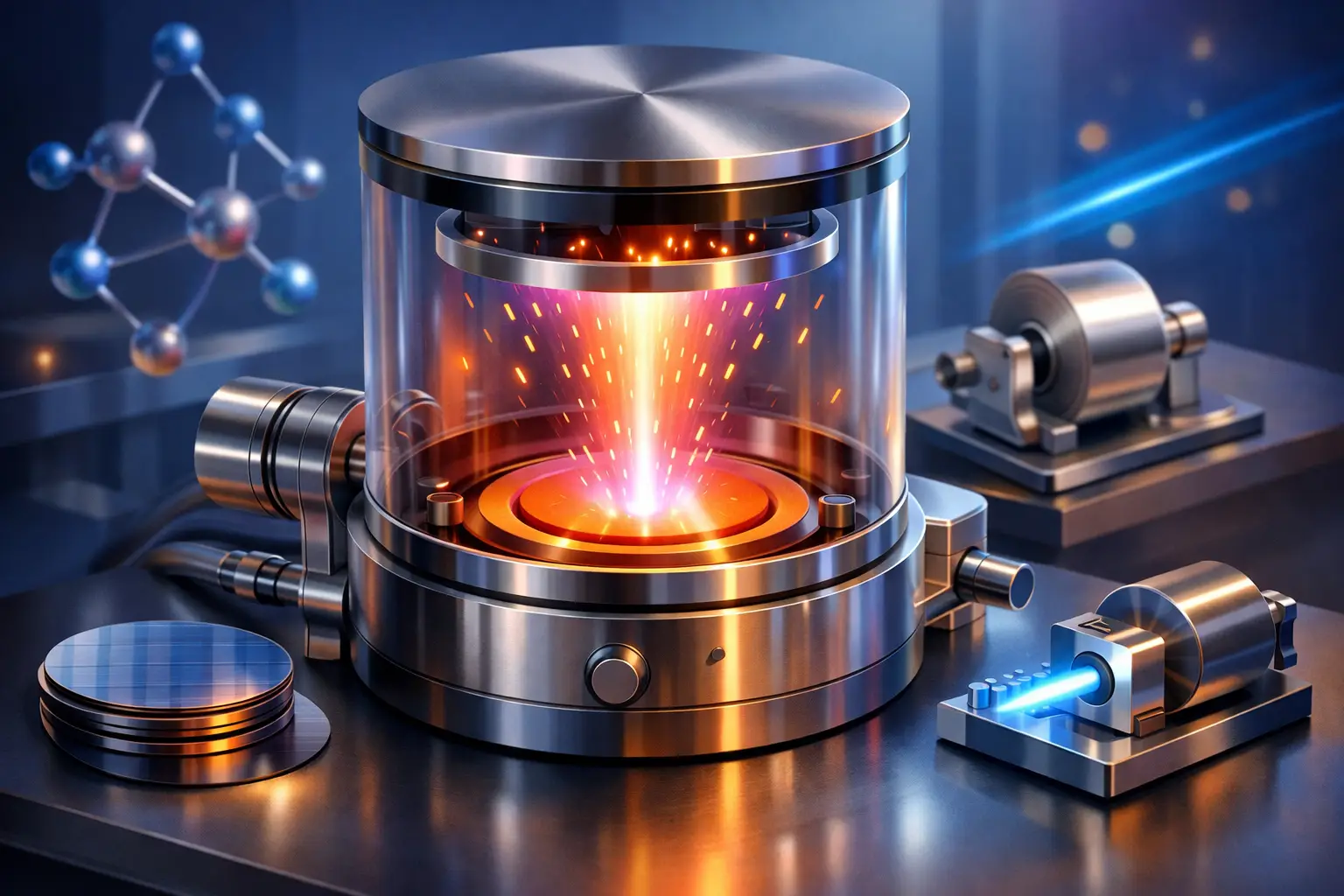
Magnetron sputtering is a vacuum-based coating process in which atoms are ejected from a solid target material and deposited as a thin film on a substrate. The driving force is a plasma, typically generated from an inert gas such as argon. Positive gas ions are accelerated towards the target, strike its surface and dislodge atoms. These atoms then travel through the vacuum chamber and condense on the component to form a coating.
What distinguishes the magnetron variant from basic sputtering is the use of a magnetic field near the target surface. This field traps electrons close to the target, increasing ionisation efficiency in the plasma. The practical effect is straightforward: higher deposition rates, more stable processing and improved control over the coating process. For industrial users, that translates into better productivity and greater process reliability.
What is magnetron sputtering used for?
Magnetron sputtering is used wherever functional thin films must be applied with tight control over thickness, composition and surface properties. Typical applications include conductive layers in electronics, barrier coatings, optical films, hard coatings for tools and components, and biocompatible or corrosion-resistant surfaces in demanding technical sectors.
In medical technology, electronics, automotive engineering, aeronautics and precision mechanics, the process is valued because it can produce dense and uniform coatings on a wide range of materials. Metals, ceramics and certain polymers can all be coated, although the exact process window depends on substrate temperature tolerance, geometry and adhesion requirements.
For technical decision-makers, the key point is that magnetron sputtering is not simply a way to put material onto a surface. It is a method for engineering surface function. Electrical conductivity, optical behaviour, friction coefficient, hardness, chemical resistance and diffusion barrier performance can all be influenced through the right combination of target material, plasma parameters and system design.
How magnetron sputtering works in practice
At process level, the sequence is relatively clear. First, the chamber is evacuated to create a controlled low-pressure environment. Then a process gas, most often argon, is introduced. A voltage is applied between the target and the chamber or substrate holder, which ignites the plasma. Argon ions are accelerated towards the target, atoms are sputtered off, and these atoms deposit on the substrate surface.
The magnetic field behind the target keeps electrons circulating near the target face rather than letting them disperse freely through the chamber. This raises plasma density in the critical region where sputtering occurs. Because more ionisation happens close to the target, the process becomes markedly more efficient than non-magnetron sputtering.
In industrial systems, additional features are often integrated to improve film performance. Substrate bias can influence ion bombardment and film density. Heating can support adhesion and crystallinity. Rotating fixtures can improve uniformity on three-dimensional parts. Reactive gases such as oxygen or nitrogen can be introduced to form oxides or nitrides directly during deposition.
This last point is especially important. In reactive magnetron sputtering, the target may be metallic, while the resulting coating becomes a compound layer such as titanium nitride or aluminium oxide. That opens up a broad design space, but it also makes process control more demanding. Gas flow balance, target poisoning and plasma stability all need to be managed carefully.
Why the process is attractive in industry
Magnetron sputtering combines several advantages that make it highly relevant for industrial coating tasks. It offers comparatively low substrate heating, precise thickness control and good reproducibility when the equipment and process are correctly configured. It also supports a broad material spectrum, from pure metals to complex ceramic films.
Another strength is coating quality. Sputtered films are typically dense and adherent, which is essential where surfaces must perform reliably under mechanical, thermal or chemical stress. For regulated industries, repeatability matters at least as much as peak performance. A coating that performs well once but drifts over time is of limited value in serial production.
There are also economic reasons for choosing this route. Magnetron sputtering can be scaled from development to industrial throughput, and it integrates well into engineered production environments. For companies evaluating whether to outsource coating or build process capability in-house, that scalability is often a decisive factor.
Where the limits begin
Even a strong process is not universal. Magnetron sputtering has clear trade-offs, and these should be understood early in project planning.
One limitation is line-of-sight deposition behaviour. Although well-designed tooling and movement systems can improve coverage, highly complex geometries, deep recesses or shadowed areas are more challenging than with some conformal coating methods. If full penetration into intricate internal structures is critical, another technology may be more suitable or a hybrid approach may be needed.
Deposition rate can also be a constraint, depending on material system and required layer thickness. For very thick coatings, other processes may be faster or more economical. Adhesion, too, is not automatic. Surface preparation, activation and interlayer design often determine whether the coating performs reliably over the long term.
There is also the question of capital intensity. Magnetron sputtering systems require vacuum technology, power supplies, cooling, gas handling and process control infrastructure. For demanding applications, the equipment must be engineered around the product and coating specification rather than selected as a generic standard machine. That is precisely where customised plant design becomes strategically relevant.
DC, RF and pulsed magnetron sputtering
Not every magnetron sputtering process is the same. The power mode depends largely on the target material and coating objective.
DC magnetron sputtering is commonly used for conductive targets such as metals. It is efficient and widely applied in industrial production. RF magnetron sputtering is better suited to insulating targets, because the alternating field avoids charge build-up on the target surface. Pulsed DC variants are frequently used to improve arc suppression and process stability, particularly in reactive deposition.
For users, the significance is practical rather than academic. The selected power mode affects deposition behaviour, coating quality, process speed and system complexity. If a specification calls for a ceramic functional layer with tight property tolerances, the process architecture must support that result from the outset.
Why process development matters more than the headline method
When companies ask what is magnetron sputtering, the underlying business question is often different: can this process deliver the coating function we need, on our component, at our production scale, with acceptable cost and reliability? The answer depends less on the name of the method than on process development and system integration.
Target material selection, substrate pretreatment, fixture design, plasma regime, coating stack architecture and quality assurance all shape the outcome. Two suppliers may both offer magnetron sputtering, yet the real-world performance of the coating can differ substantially. This is especially true for components with tight tolerances, mixed materials, critical adhesion requirements or regulatory constraints.
For that reason, successful projects usually begin with the application, not the machine. The surface challenge must be defined clearly: wear reduction, corrosion protection, conductivity, dielectric behaviour, biocompatibility or optical function. Only then does it make sense to configure the process window and, where relevant, the plant architecture.
What technical buyers should evaluate
If magnetron sputtering is being considered for a product or production line, it is worth assessing more than nominal coating data. Decision-makers should look at achievable uniformity on the actual component geometry, adhesion under realistic operating conditions, batch-to-batch repeatability, cleanliness standards and compatibility with downstream manufacturing steps.
It is equally important to clarify whether the requirement is best served by contract coating, pilot-scale development or a custom-built coating system integrated into in-house production. In sophisticated industrial settings, the coating process is often only one part of a larger chain that includes cleaning, handling, inspection and validation. A coating technology creates lasting value when it fits that chain reliably.
This is where an engineering-driven partner can make a measurable difference. Companies such as NTTF Coatings work at the intersection of thin-film process expertise, application-specific development and custom system design – a combination that becomes particularly valuable when standard solutions do not meet functional or regulatory demands.
Magnetron sputtering is best understood not as a single answer, but as a highly controllable platform for building surface function with precision on an industrial scale. When the coating task is defined clearly and the process is developed around the application, it becomes a powerful tool for improving component performance where small surface changes have large technical consequences.
