
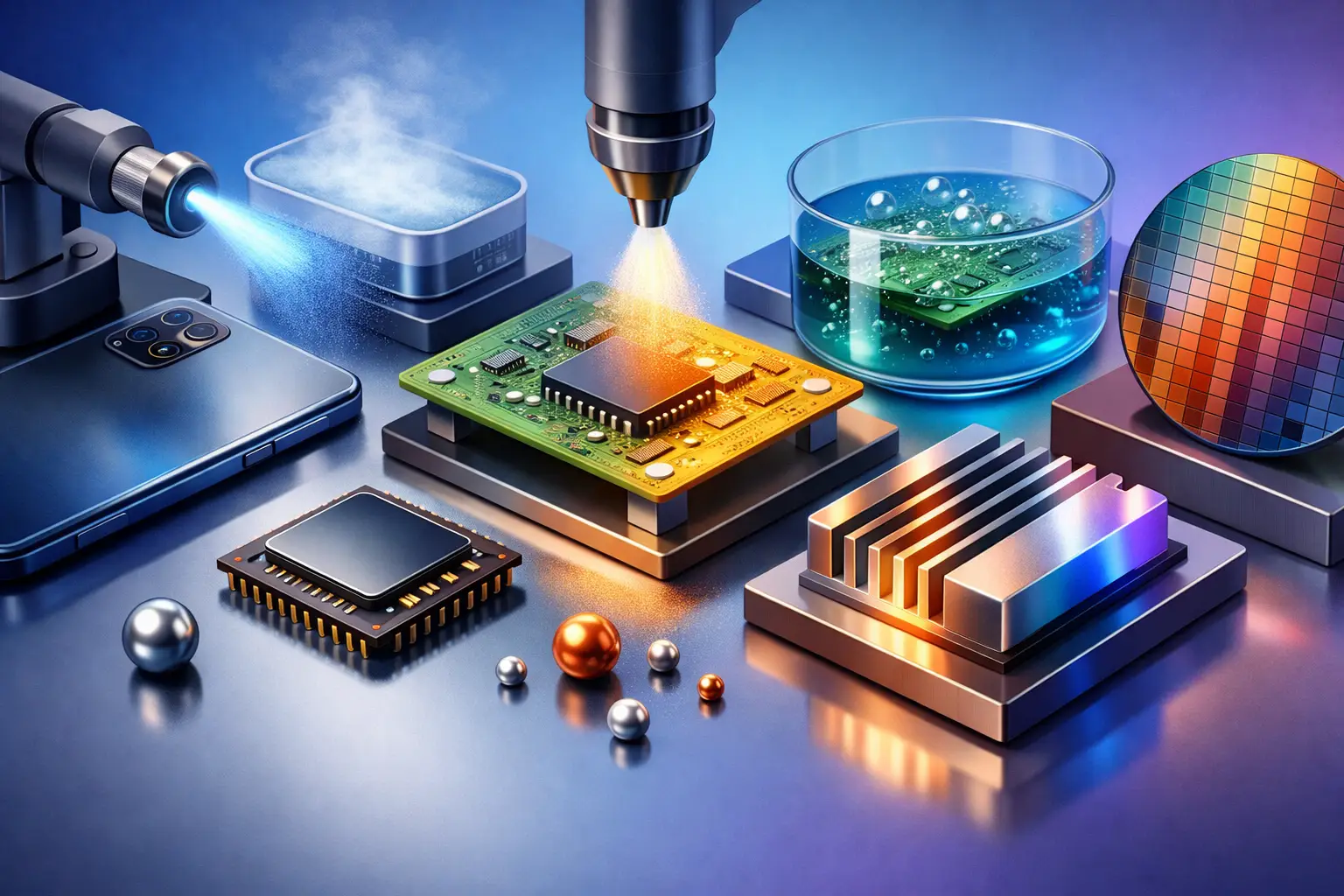
A control board that performs flawlessly in the lab can fail early in the field for one simple reason: its surface was never engineered for the real operating environment. Moisture ingress, ionic contamination, outgassing, abrasion, aggressive media and high-voltage stress all act at the surface first. That is why selecting the best surface treatments for electronics is less about adding a final protective layer and more about defining long-term function, reliability and manufacturability from the outset.
For technical decision-makers, the real question is not which treatment sounds most advanced. It is which process matches the substrate, the geometry, the required barrier performance, the electrical function, the regulatory framework and the target cost over the product lifecycle. In electronics, a coating that is excellent for one assembly can be unsuitable for another.
What makes the best surface treatments for electronics?
The answer depends on what the surface must achieve. In some applications, the primary requirement is corrosion protection against humidity, salt or process chemicals. In others, it is dielectric insulation at thin layer thicknesses, reduced friction on moving contact elements, improved adhesion before bonding or encapsulation, or a defined biocompatible interface for medical electronics.
A technically sound selection always starts with the load profile. Electronics in automotive engine compartments face a different combination of heat cycling, vibration and chemical exposure than sensor systems in medical devices or avionics assemblies in low-pressure environments. The best treatment is therefore the one that delivers the required functional performance with stable process control and reproducible quality in series production.
Parylene coatings: when uniform dielectric protection matters
Parylene is often one of the strongest candidates when electronic components require highly uniform, pinhole-free conformal coverage. Because the coating is deposited from the gas phase, it can cover complex geometries, sharp edges, cavities and fine structures with remarkable consistency. This matters for miniaturised electronics, densely packed assemblies and sensitive sensor systems where conventional liquid-applied coatings may struggle with shadowing, pooling or edge thinning.
From a functional standpoint, Parylene combines strong dielectric properties with excellent barrier behaviour against moisture and many chemicals. It is also attractive where low layer thickness is essential. A comparatively thin coating can already provide high-value insulation and environmental protection without adding significant mass or altering component dimensions.
That said, Parylene is not a universal answer. Process preparation is critical, particularly surface cleanliness and adhesion promotion where needed. Certain designs may also require selective masking, which must be engineered carefully for repeatable production. For high-volume programmes, throughput and fixture strategy also deserve attention early in the project phase.
Plasma treatment: often the decisive step before the coating
Plasma treatment is sometimes overlooked because it is not always the final functional layer. In practice, it is frequently one of the most decisive process steps in the chain. Plasma can activate surfaces, remove organic residues, improve wettability and create the conditions needed for reliable adhesion of subsequent coatings, bonding agents or printing processes.
For electronics manufacturers, this is highly relevant wherever adhesion stability determines field performance. Poor adhesion can compromise not only coating durability but also sealing, overmoulding and bonded assembly integrity. Plasma processes can also be tailored to delicate substrates and fine structures, making them suitable for sensitive components where wet-chemical cleaning would be less controlled.
Its limitation is equally clear: plasma alone does not replace every protective coating. If the application requires a defined moisture barrier, dielectric layer or wear-resistant film, plasma is usually part of the surface engineering strategy rather than the complete solution.
PVD coatings: functional thin films for specific electronic demands
Physical vapour deposition, or PVD, becomes relevant when electronics require more than environmental protection. PVD processes can create thin films with defined electrical, optical, tribological or barrier properties. Depending on the coating material and architecture, they can support conductive pathways, reflectivity control, wear reduction or improved resistance against certain media.
In electronic systems, PVD is particularly useful where the surface must perform actively rather than simply act as a passive shield. Connectors, contact areas, housings, sensor elements and specialised functional layers can benefit from tightly controlled thin-film deposition. The strength of PVD lies in precision and tunability.
The trade-off is that line-of-sight deposition can limit coverage on highly complex three-dimensional geometries. If an assembly has deep recesses or intricate shadowed features, the achievable uniformity may not match a conformal vapour polymer process such as Parylene. This does not diminish PVD’s value, but it does mean geometry and fixturing must be considered early.
CVD and hybrid processes: when performance requirements overlap
Chemical vapour deposition, along with hybrid thin-film strategies, is especially relevant when applications demand a combination of properties that a single standard process cannot deliver. Some electronics need a barrier layer, electrical insulation, chemical resistance and a precise mechanical surface response in one integrated concept. In these cases, multi-step or hybrid systems often offer the most reliable route.
Hybrid approaches are attractive because they allow engineers to separate functions deliberately. One layer can improve adhesion, another can deliver barrier performance, and a final layer can tailor friction, biocompatibility or electrical behaviour. For highly regulated sectors such as medical technology, aerospace or defence, that level of control can be more valuable than choosing a nominally cheaper single-layer option that leaves performance gaps.
The cost and qualification effort are usually higher. However, when component failure carries substantial warranty, downtime or compliance risk, the economics often favour the more precise process chain.
How to compare the best surface treatments for electronics
A useful comparison starts with five questions. What failure mode must be prevented first? Which substrates are involved? How complex is the geometry? What are the production volumes? And what qualification evidence will customers or regulators expect?
If the main challenge is uniform conformal insulation and moisture protection on complex assemblies, Parylene is often difficult to beat. If adhesion issues sit at the root of downstream failures, plasma treatment may deliver the greatest benefit even when it is not visible in the final product. If a surface needs specific conductive, optical or wear-related properties, PVD is frequently the more appropriate technology. If the component must satisfy several demanding functions at once, CVD or hybrid architectures deserve serious consideration.
It also helps to distinguish prototype success from industrial viability. A treatment that performs well on a few sample parts may not scale efficiently if masking effort, takt time, inspection complexity or maintenance demands become excessive in series production. For this reason, process design and coating design should never be separated.
Industry-specific priorities change the selection
In medical electronics, biocompatibility, sterilisation resistance and long-term stability are often central. For automotive electronics, temperature cycling, splash water, fuels, oils and vibration may dominate. In aerospace and defence, outgassing behaviour, reliability under extreme environmental stress and traceable process control carry particular weight. Industrial automation systems may prioritise chemical resistance, electrical insulation and cost-stable repeatability across long product runs.
This is where a standard catalogue approach tends to fail. Surface treatment selection for electronics works best when process parameters, masking concepts, substrate behaviour and inspection criteria are developed around the application rather than imposed on it.
Why process integration matters as much as coating performance
The best surface treatment can underperform if it is introduced poorly into production. Pre-treatment, handling, cleanliness, fixturing, masking, curing or post-process inspection all influence the final result. In many projects, the real technical value lies not only in the coating chemistry but in building a stable, reproducible process window around the component.
For companies deciding between outsourcing and in-house capability, this point is especially relevant. Contract coating offers speed, specialist expertise and reduced capital expenditure. An in-house system can make sense where volumes are high, process control must remain internal or coating is strategically embedded in product manufacturing. Providers with both coating expertise and custom equipment capability, such as NTTF Coatings GmbH, are well placed to support that decision on a technically grounded basis rather than through a one-size-fits-all recommendation.
Surface engineering in electronics is rarely about choosing the most familiar label. It is about selecting the process that protects function under real conditions, scales with production and remains stable when tolerances tighten. The right answer is usually found where material science, component design and manufacturing reality meet.
