
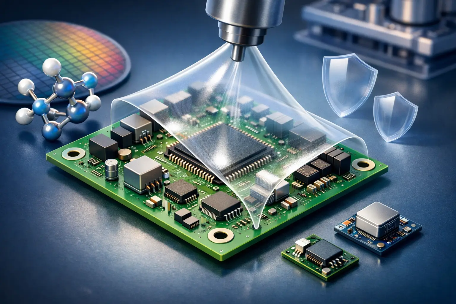
A control module can pass electrical testing on Friday and fail in the field months later for a reason that is difficult to see: moisture has reached an unprotected edge, ionic residues have initiated leakage, or corrosion has begun beneath a connector. This parylene coating case study for electronics examines how a vapour-deposited conformal coating can address such failure mechanisms without compromising the function, geometry or accessibility of sensitive assemblies.
The scenario is representative of industrial electronics projects in which a standard coating approach has reached its limits. It is not a claim about a single customer programme or a universal recipe. The technical result always depends on component design, materials, operating environment, cleanliness requirements and the qualification route.
The electronics challenge behind the case study
The application considered here is a compact electronic control assembly installed in an environment subject to humidity cycling, temperature variation and intermittent exposure to corrosive contaminants. The assembly contains populated printed circuit boards, fine-pitch components, solder joints, connector regions and areas where low leakage current is essential to measurement accuracy.
The initial protection concept used a conventional liquid conformal coating. Coverage on broad, accessible surfaces was acceptable, but the process created several concerns. Film thickness varied around component edges, sharp geometries and densely populated regions. Shadowed zones beneath components were difficult to protect reliably. The liquid process also introduced questions around solvent handling, curing, masking residue and inspection of critical interfaces.
These issues matter because electronics failures rarely occur at the most visible surface. They often begin where a coating has thinned, pulled away, trapped contamination or failed to cover a narrow gap. For assemblies that must remain stable over long service intervals, the coating is not an isolated production step. It is part of the electrical and environmental design.
Why Parylene was selected for evaluation
Parylene is deposited from the vapour phase in a vacuum process. The precursor is converted into reactive monomer molecules that polymerise directly on exposed surfaces, forming a highly conformal polymer film. Unlike a liquid coating, the deposited material does not need to flow into fine structures. This is particularly relevant for component edges, narrow clearances, wire bonds, leads and complex three-dimensional geometries.
For this electronics application, the evaluation focused on four properties: uniform coverage, dielectric performance, barrier behaviour against moisture and corrosive media, and low mechanical loading on sensitive parts. Parylene can provide these characteristics at film thicknesses measured in micrometres. That matters where mass, clearance and heat-transfer constraints leave little room for thick protective layers.
However, thin does not automatically mean suitable. The Parylene type, target thickness, deposition rate, substrate condition and masking concept must be matched to the actual use case. A coating designed primarily for moisture protection may require different optimisation from one intended to maintain electrical insulation at elevated temperature or resist aggressive process media.
Parylene coating case study: defining the process window
The development work began before the first production deposition. The assembly was reviewed as a system rather than as a generic PCB. Particular attention was paid to connector contacts, test points, heat-generating components, elastomeric parts, labels, optical elements and locations where subsequent bonding or soldering might be required.
Surface condition determines coating performance
Parylene reproduces the surface it covers with exceptional fidelity. This is an advantage on clean, stable surfaces, but it also means that flux residues, handling contamination, silicone transfer and absorbed moisture cannot be ignored. A high-quality film deposited over ionic contamination does not remove the underlying risk of electrochemical migration.
The pre-treatment strategy therefore included defined cleaning, controlled drying and handling measures. Depending on the substrate and contamination profile, plasma activation can be used to improve surface condition and adhesion behaviour. The purpose is not to apply a standard pre-treatment to every board. It is to establish a reproducible condition that supports the required coating performance.
Masking is a functional design task
Not every surface should receive Parylene. Electrical contacts, press-fit areas, optical windows, thermal interfaces and grounding locations may need to remain coating-free. In this case, the masking concept was developed alongside the assembly design and manufacturing sequence.
This prevents a common late-stage problem: a coating performs well environmentally but obstructs a required electrical or mechanical interface. Masking materials must withstand vacuum conditions, release cleanly and maintain positional accuracy. Their design also influences process throughput and the feasibility of automation.
Thickness is a controlled compromise
A thicker film can improve barrier performance in some conditions, yet it may create drawbacks. It can alter tolerances at connectors, increase stress at sharp edges, affect thermal paths or make rework more demanding. Conversely, an excessively thin layer may not provide sufficient protection for the intended exposure profile.
The selected thickness should therefore follow a risk-based assessment, supported by test data rather than assumptions. In demanding programmes, thickness mapping on representative geometries helps confirm that nominal settings translate into coverage where it is needed. The goal is repeatable protection, not the highest possible micrometre value.
Qualification must reflect the real failure mechanism
Visual inspection alone cannot validate a protective coating for critical electronics. A glossy surface may conceal incomplete masking, weak adhesion, contamination or insufficient coverage in inaccessible regions. The qualification plan for the representative assembly combined process controls with application-related testing.
Electrical insulation and leakage behaviour were assessed before and after environmental exposure. Temperature-humidity cycling was used to challenge the coating-substrate system under changing conditions. Where corrosive exposure was relevant, test conditions were chosen to represent the expected contamination mechanism rather than relying solely on generic climate tests.
Adhesion evaluation was also necessary, but its interpretation required care. Adhesion is influenced by laminate chemistry, solder mask, component packaging, cleaning history and the presence of surface treatments. A result from one coupon cannot automatically be transferred to every material in the bill of materials.
For regulated or safety-relevant electronics, documentation is as important as the physical test. Defined batch traceability, deposition parameters, masking instructions, inspection criteria and release records create the basis for reproducibility. This is where a technically capable coating process becomes an industrially controlled process.
From pilot coating to serial production
The pilot phase confirmed that Parylene could protect the relevant geometry without interfering with designated interfaces. The next question was economic and operational: should the coating remain an external service, or should it be integrated into the customer’s own production?
For low to medium volumes, changing variants or development programmes, industrial contract coating can reduce capital commitment and accelerate qualification. It allows the manufacturer to establish the coating specification while retaining flexibility for design changes. It is particularly useful when specialised process knowledge and metrology are needed but continuous plant utilisation is not yet justified.
For high-volume products or strategically sensitive manufacturing, an in-house system may be the stronger option. The decision is not based on annual volume alone. It also depends on batch size, required turnaround, product mix, cleanroom integration, traceability demands, maintenance capability and the cost of production interruption.
A custom-designed Parylene plant can be configured around these parameters. Chamber size, loading concept, vacuum architecture, precursor handling, process monitoring and automation should support the actual production model. NTTF Coatings GmbH approaches this stage as an engineering task: coating performance, operator safety, maintainability and quality assurance must work together in one validated process chain.
What this case study changes in electronics design
The main lesson is that Parylene should not be specified as a final protective layer after the electronics design has been frozen. Its value is greatest when coating, geometry, interfaces and validation are considered together. Early involvement makes it possible to define keep-out zones, material restrictions, cleaning requirements and test methods before they become expensive changes.
It also avoids overpromising. Parylene offers highly conformal, pinhole-free deposition under correctly controlled conditions, but it is not a substitute for sound enclosure design, contamination control or appropriate component selection. If the assembly experiences immersion, extreme abrasion, exceptional heat or repeated connector mating, further measures may be required.
For electronic assemblies operating where failure is costly, the most useful question is not simply whether Parylene can be applied. It is whether the coating system has been engineered, qualified and scaled to protect the precise interfaces on which the product depends.
