
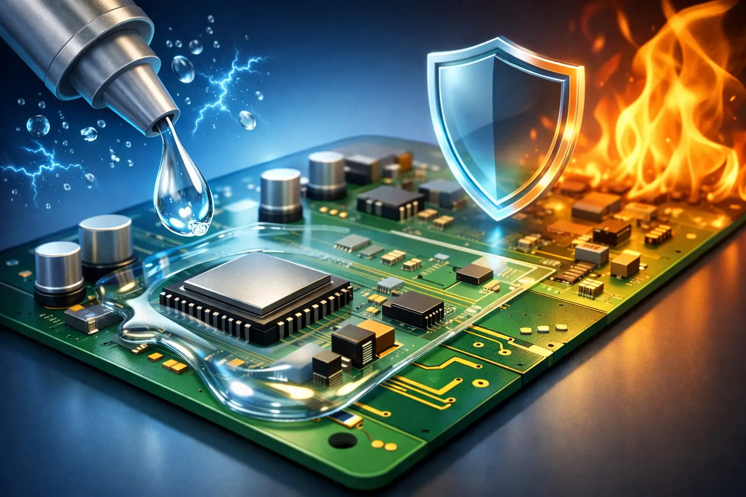
A PCB can pass electrical test at the end of production and still fail months later because moisture, ionic contamination or corrosive gases reach a critical surface. The best barrier coatings for PCBs are therefore not selected by nominal film thickness alone. They must protect the actual assembly geometry, preserve electrical function and remain reliable through the temperature, chemical and mechanical loads of service.
For electronics used in medical devices, automotive systems, aerospace equipment, industrial controls or defence applications, coating selection is a systems decision. Substrate material, component density, clearance requirements, operating voltage, rework strategy and production volume all influence the right answer.
What a PCB barrier coating must achieve
A barrier coating separates sensitive conductors, solder joints and components from their environment. In practice, the primary threat is often not liquid water but the combination of humidity, condensed moisture and ionic residues. This combination can initiate electrochemical migration, corrosion and leakage currents between closely spaced conductors.
The coating must also tolerate the operating environment. Thermal cycling can stress the interface between coating and board. Vibration can expose weak adhesion. Fuels, cleaning agents, skin oils or process media can attack susceptible polymers. At higher frequencies or voltages, dielectric properties and coating uniformity become electrical design parameters rather than secondary details.
A useful barrier system therefore needs more than a low moisture transmission rate. It requires controlled adhesion, complete coverage of critical regions, appropriate dielectric behaviour and a process that delivers reproducible film quality.
Best barrier coatings for PCBs: the main options
There is no universal best material. Conventional conformal coatings, vapour-deposited polymer films and inorganic or hybrid thin films each solve different protection problems.
Acrylic conformal coatings
Acrylic systems are widely used where moderate environmental protection, straightforward processing and practical rework are priorities. They are typically applied by spraying, dipping or selective coating and can offer a cost-effective solution for indoor industrial electronics.
Their limitation is barrier performance in severe humidity, chemical exposure and prolonged outdoor service. Coverage around fine-pitch components, connector interfaces and sharp edges also depends heavily on viscosity, application settings and curing control. Acrylic may be entirely appropriate for a controlled environment, but it should not be assumed to provide long-term protection in a condensation-prone assembly.
Silicone conformal coatings
Silicone coatings are valued for flexibility and resistance to thermal cycling. They suit assemblies exposed to wide temperature ranges, vibration or elevated operating temperatures, particularly where a relatively soft coating is advantageous.
However, silicone is not automatically the strongest choice for moisture or chemical barrier performance. Its permeability can be higher than that of denser polymer films, and contamination control is essential because silicone residues can complicate subsequent bonding, painting or rework. The right silicone formulation can be highly effective, but its benefits should be matched to thermal-mechanical requirements rather than treated as a default answer to every corrosion risk.
Polyurethane and epoxy systems
Polyurethane coatings provide good mechanical durability and chemical resistance in many industrial environments. They are often selected for boards facing oils, fuels or harsher handling conditions. Epoxy-based coatings can deliver a hard, chemically resistant layer and are useful where abrasion resistance and structural rigidity matter.
The trade-off is reduced reworkability and, in some cases, greater stress during thermal cycling. A hard coating can protect a board well while placing additional strain on components, solder joints or interfaces with differing coefficients of thermal expansion. These materials demand careful qualification when assemblies include large ceramic capacitors, fine-pitch devices or sensitive sensors.
Parylene coatings
Parylene is frequently among the strongest candidates when a PCB requires highly uniform, thin and conformal protection. Deposited by a room-temperature chemical vapour deposition process, Parylene polymerises from the vapour phase and coats exposed surfaces, edges and complex three-dimensional geometries with exceptional conformity.
This is particularly relevant for densely populated boards, sharp conductor edges, fine-pitch components and areas beneath or around packages where liquid-applied coatings may thin, bridge or leave shadowed regions. Depending on the Parylene type, the coating can provide excellent dielectric performance, low moisture permeability, chemical resistance and stable protection at thicknesses commonly measured in micrometres rather than tens or hundreds of micrometres.
Parylene C is a well-established choice for moisture and corrosion protection. Parylene N may be selected where lower dielectric constant is significant, while high-temperature or UV-exposed applications may call for specialised fluorinated variants. The designation alone is not enough: board cleanliness, masking, adhesion promotion and film thickness must be engineered around the application.
Plasma, PVD and hybrid thin-film barriers
Plasma processes can modify PCB surfaces at a molecular scale, improving surface cleanliness, activation and adhesion before a subsequent coating step. Plasma-polymerised layers may also add hydrophobic or oleophobic functionality where very thin functional films are required.
PVD coatings and inorganic barrier layers can provide highly targeted surface properties, but their line-of-sight nature limits their suitability as a stand-alone protective layer for complex, fully populated PCBs. Hybrid systems can combine an inorganic barrier layer with a conformal polymer top layer, balancing chemical resistance, dielectric performance and mechanical tolerance. Such systems are technically demanding, yet valuable where conventional conformal coating reaches its limits.
Conformity matters more than a nominal thickness
A 50-micrometre coating is not necessarily more protective than a 10-micrometre film. If a liquid coating pulls away from an edge, forms bubbles, leaves thin spots or traps contamination, its local barrier performance can fail at precisely the points where the assembly is most vulnerable.
Vapour-deposited Parylene addresses this issue through its ability to follow the PCB topography. That does not eliminate all failure modes. Coating coverage is only useful where the board is clean, surfaces are compatible and specified areas have been properly masked. Connectors, test pads, heat-dissipating zones, optical surfaces and moving contacts may require selective exclusion from the process.
For this reason, coating design should begin with a coverage map. It identifies every region that must be protected, every area that must remain uncoated and every transition where a coating edge could become a reliability risk.
Adhesion and cleanliness decide long-term performance
Many apparent coating failures are interface failures. Flux residues, fingerprints, mould-release agents, moisture absorbed by the substrate and insufficient surface energy can all weaken adhesion. The resulting defect may be difficult to detect initially, then propagate under humidity and temperature cycling.
A controlled cleaning programme, drying step and surface preparation method are therefore central to barrier performance. Plasma activation can be particularly effective where the PCB finish, component materials or process residues create adhesion uncertainty. Adhesion promoters may also be necessary, but they should be assessed for compatibility with the coating chemistry and the required service life.
Qualification should test the complete stack: laminate, solder mask, metallisation, components, residues, surface preparation and coating. Testing an isolated coupon gives useful material data, but it does not fully represent the assembly that will enter production.
Electrical requirements cannot be treated as an afterthought
For low-voltage electronics with generous conductor spacing, the dielectric influence of a coating may be modest. For high-impedance circuits, high-voltage assemblies, RF modules and miniature sensor electronics, it can be decisive. Dielectric constant, dissipation factor, insulation resistance and the risk of ionic migration should be evaluated against the real circuit design.
Thickness also has electrical consequences. A thicker coating can increase protection in some situations, but may alter capacitance, impede heat transfer or complicate inspection and repair. In RF applications, coating placement around antenna structures, resonators and controlled-impedance features requires explicit design review.
From laboratory result to repeatable production
A coating is only as reliable as the process used to apply it. The critical controls include incoming board condition, bake-out, masking accuracy, chamber loading, deposition parameters, cure or post-treatment conditions, film-thickness verification and visual inspection criteria.
For regulated or safety-relevant electronics, traceability should connect material batches, process parameters and inspection results to each production lot. Where a product must scale from prototypes to serial manufacture, the process window needs to be defined early. A coating that performs well on a few hand-prepared samples may not be stable when board mix, loading density and throughput increase.
NTTF Coatings develops coating routes and equipment concepts around these interactions, including Parylene deposition, plasma preparation and hybrid thin-film approaches. This is most valuable when protection performance and production integration must be established together rather than treated as separate projects.
A practical selection route
The selection process should start with the failure mechanism, not with a preferred coating family. Define whether the dominant risk is humidity, salt mist, condensation, chemicals, thermal cycling, vibration, high voltage or contamination. Then assess board geometry, component restrictions, masking needs, inspection method and repair requirements.
Next, compare candidate systems using representative assemblies and realistic exposure conditions. Measure insulation resistance and adhesion after ageing, inspect edges and hidden areas, and evaluate whether the coating affects thermal management or electrical behaviour. Finally, verify that the chosen process can be held within defined limits at the intended production volume.
The most effective PCB barrier coating is the one that protects the vulnerable interfaces without creating a new limitation in manufacturing, electrical performance or serviceability. Starting with the failure mechanism and qualifying the full assembly turns coating from a final protective layer into an engineered reliability function.
