
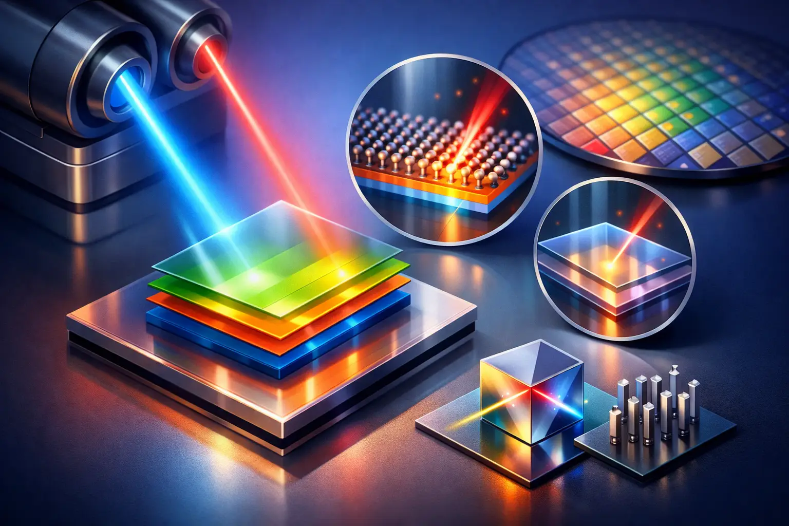
A component rarely fails because its bulk material is intrinsically unsuitable. More often, failure begins at the surface: moisture reaches an electronic assembly, friction alters a precision mechanism, an implant-facing surface causes an unwanted biological response, or a barrier layer develops microscopic defects. Thin films address precisely this interface. They add a functional layer, often only nanometres to micrometres thick, without fundamentally changing the geometry or mechanical purpose of the underlying component.
For technical decision-makers, the value of thin films is therefore not their low thickness alone. It is the ability to define surface behaviour with high precision: electrical insulation or conductivity, chemical resistance, reduced friction, diffusion barrier performance, adhesion, optical function or biocompatibility. The right coating turns an existing material into a component suited to a far more demanding operating environment.
What makes thin films technically different?
A thin film is a deliberately deposited material layer whose function is governed not only by its chemistry, but also by its microstructure, thickness uniformity, adhesion and interface with the substrate. At these dimensions, minor variations can have a major effect. A local discontinuity may compromise corrosion protection. Internal stress may cause cracking or delamination. An unsuitable pre-treatment can leave a coating technically sound in principle but unreliable in series production.
This distinguishes functional thin-film technology from a simple finishing operation. The coating must be developed as part of the component system. Substrate material, geometry, surface condition, handling, cleaning, masking, coating method and subsequent validation all influence the final result.
For example, a polymer coating may be selected for excellent dielectric strength and conformal coverage on densely populated electronics. A PVD layer may be chosen for hardness, wear resistance or a defined electrical property. CVD and plasma-based processes offer further options where chemical bonding, barrier behaviour or surface activation are decisive. No process is universally superior. The appropriate choice depends on the failure mechanism that must be controlled.
Thin films are designed around the application
The first technical question should not be, “Which coating is available?” It should be, “What must the surface achieve throughout the component’s service life?” This shift prevents a common development error: selecting a material based on a single headline property while overlooking process and operating conditions.
In medical technology, a thin film may need to combine biocompatibility with chemical stability, dielectric protection and reliable coverage of intricate geometries. In automotive electronics, resistance to humidity, temperature cycling, ionic contamination and vibration can be more relevant than nominal coating hardness. In aerospace and defence applications, stringent traceability, demanding environmental exposure and controlled material selection may set the framework. For machinery components, the priority may be reduced wear, lower friction or protection against aggressive media.
The required performance must also be quantified. Terms such as “corrosion-resistant” or “electrically insulating” are insufficient specifications on their own. Relevant questions include the expected medium, temperature range, exposure duration, voltage level, permissible leakage current, mechanical loading and acceptable defect rate. A measurable requirement creates a basis for process development, testing and quality assurance.
The substrate is part of the coating system
Metal, glass, ceramic, polymer and composite substrates each present different challenges. Their surface energy, roughness, thermal expansion and chemical condition determine how a film nucleates, grows and adheres. Even components made from the same nominal alloy may behave differently after machining, cleaning, heat treatment or storage.
Complex geometry adds another layer of consideration. Cavities, edges, undercuts, sharp radii and blind holes do not receive every coating in the same way. Parylene, for instance, is valued for highly conformal deposition, making it suitable for complex assemblies where line-of-sight methods have limitations. PVD processes can provide highly functional layers, but their deposition characteristics must be assessed against component orientation and shadowing effects. The geometry should therefore influence the process concept from the outset rather than become a late-stage constraint.
Deposition method determines performance and scalability
Thin-film technologies are often grouped by their deposition principle, but the practical distinction lies in the resulting layer and its reproducibility. Physical vapour deposition, chemical vapour deposition, plasma processes and hybrid approaches can each produce high-value functional surfaces. Their suitability depends on the material system, the component, the target properties and the intended production volume.
PVD is particularly relevant where hard, dense or conductive layers are required. Depending on process design, it can support wear protection, decorative functional finishes, optical effects or electrical applications. The trade-off is that coating distribution on complex three-dimensional parts requires careful chamber design, fixturing and parameter control.
CVD uses reactive precursors to form a layer on the substrate. It enables material systems and film properties that are difficult to achieve by purely physical deposition. Process temperature, precursor chemistry and reaction control are central considerations, particularly for temperature-sensitive substrates.
Plasma technology serves both as a coating route and as a crucial preparation step. Plasma cleaning and activation can remove organic residues, increase surface energy and improve adhesion before subsequent coating. In some applications, this pre-treatment is the difference between nominal performance in a laboratory test and stable performance over a production lifetime.
Parylene deposition occupies a distinctive role in applications requiring pinhole-minimised, conformal polymer films. Its ability to coat edges and complex topographies makes it especially relevant for electronics, sensors, medical components and assemblies exposed to moisture or chemicals. Yet conformality does not eliminate the need for engineering discipline. Material selection, layer thickness, masking strategy, outgassing behaviour and verification remain essential.
Process development must precede series production
A successful thin-film project usually moves through a defined sequence: feasibility assessment, sample preparation, coating trials, functional testing, process optimisation and transfer to serial production or an in-house system. Skipping steps can appear economical at first, but it often shifts risk into qualification, field performance or yield losses.
The feasibility phase should consider more than whether a coating can be applied. It should establish whether the required function can be achieved consistently on the real component, with its actual tolerances and material condition. Test coupons are useful, but they do not always replicate the thermal mass, edge geometry, contamination risk or handling conditions of a finished assembly.
For regulated sectors, qualification should reflect the component’s intended use. This may include adhesion assessment, coating thickness measurement, electrical tests, chemical exposure, climate cycling, corrosion testing, particle analysis or biocompatibility-related evaluation. The test plan should be proportionate to the risk. A coating on a non-critical enclosure demands a different evidence base from one on a medical device component or a safety-relevant electronic module.
Reproducibility is an engineering outcome
Reproducible quality does not result from a single final inspection. It comes from controlling the entire process chain: incoming component condition, cleaning, loading density, masking, chamber parameters, deposition time, maintenance and inspection methods. Traceable process data provides the basis for identifying variation before it becomes a quality issue.
This is particularly relevant when a coating process moves from low-volume development into serial manufacture. A recipe that works for a few prototype parts may require different tooling, loading concepts or automation for production quantities. The coating system must be designed for throughput without sacrificing layer uniformity or access to critical surfaces.
For companies considering internal coating capability, equipment selection should begin with the product and process specification, not with a standard machine configuration. Chamber size, vapour flow, vacuum performance, handling, fixture design, cleaning integration and data capture should reflect the actual component portfolio. NTTF Coatings develops coating solutions and customised systems around this principle: process capability and equipment design must support one another.
Questions worth resolving before selecting a coating partner or system
The following points help turn a broad surface requirement into an implementable technical brief:
- Which failure mode must the thin film prevent, reduce or delay?
- Which substrate materials, geometries and component cleanliness levels are present?
- Which operating media, temperatures, voltages and mechanical loads will occur?
- Which evidence is required for release, traceability and regulatory compliance?
- Is the requirement limited to prototype quantities, or must it support a controlled series process?
Answers to these questions reveal the real trade-offs. A thicker layer may improve barrier performance but affect dimensions or flexibility. A harder film may improve wear resistance while increasing sensitivity to substrate deformation. A highly specialised process may offer exceptional performance but require more stringent preparation and higher investment. Good thin-film engineering makes these compromises explicit and manages them early.
Surface function becomes a design parameter
Thin films are most effective when they are specified at the same stage as material selection, tolerances and assembly methods. Treated as an afterthought, they can expose avoidable issues in geometry, cleaning or validation. Integrated early, they allow engineers to tailor component behaviour at the surface while retaining the properties and cost advantages of the base material.
The most useful next step is not to select a technology by name, but to define the operating conditions and the failure that cannot be allowed to occur. From there, a coating process can be engineered with the precision that demanding components require.
